Research Highlights
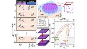
The communications blackout problem encountered by objects rapidly traveling in atmosphere can be mitigated via the application of magnetic fields. Traditional (electro-)magnets used to generate strong out-of-plane fields to magnetize plasma sheaths can be large and heavy, limiting the benefits of the approach. This article investigates the potential use of magnetic material sheets magnetized in-plane to reduce material size requirements and make use of the material’s natural shape anisotropy. Via frequency bandwidth analysis, the existence of open communication bands due to applied in-plane magnetic fields is revealed. Numerical solvers are formulated to compute (i) the varying fields applied in 3D space from source magnetization regions and (ii) signal attenuation through magnetized plasmas. Performing three numerical studies, it is found that the sizes and locations (in frequency space) of opened windows depend on the plasma profile, the transmitter location, and the material shape, and the magnetic configurations, which offer the greatest reduction in signal attenuation, can often be unintuitive. In addition, it is shown that it is possible to use arrays of smaller magnetic elements to emulate the performance of bulk material, enabling the use of modern thin-film magnetic materials. The presented analysis and numerical studies show that thin-film magnets are expected to be able to open windows to overcome communication blackout.


Analog sensing devices that exhibit artificial synaptic behavior offer a promising path toward scalable and energy-efficient environmental sensing. In this work, we report graphene-based, leaf-gated in-sensor compute devices for plant hydration monitoring that are capable of both hydration sensing and synapse-like conductance modulation. These devices measure plant water content through trends in channel conductance while simultaneously encoding memory-like states in response to electrical stimulation. Conductance changes track hydration-dependent ion mobility in the leaf with higher (lower) updates in hydrated (dehydrated) states. Devices show linear potentiation and depression and short-term memory retention, supporting their suitability for neuromorphic edge applications. When deployed on Monstera leaves, the devices maintain ultralow power operation (23 aJ/μS write energy/conductance update and 0.23 μW read power) and minimal weight (9 mg) and cause no disruption to plant physiology. By integration of computation and sensing into a single biocompatible platform, this approach minimizes data transmission requirements and enables real-time, long-term hydration monitoring.
Find the link here:
https://pubs.acs.org/doi/10.1021/acs.nanolett.5c05507

Near-infrared (NIR) photothermal therapy (PTT) using nanomaterials is a promising strategy for selective cancer treatment. We report two tin-based two-dimensional (2D) nanoflakes─defective SnS2 (SnS2–x) and mixed-phase SnOx─synthesized via top-down ultrasonication and electrochemical exfoliation with oxidation, respectively. Both nanoflakes have thicknesses below 20 nm, and their lateral sizes (<400 nm) were confirmed by AFM, DLS, atomic force microscopy, dynamic light scattering, and transmission electron microscopy (TEM). Despite a similar optical band gap (∼1.89 eV), SnO2 nanoflakes display a significantly enhanced NIR photothermal performance under 810 nm light emitting diode (LED) irradiation. A 3 mg/mL SnOx dispersion increases in temperature by ∼19 °C after 30 min, and a 0.25 mg/mL sample achieves a photothermal conversion efficiency of 93%. X-ray photoelectron spectroscopy and TEM analyses show that SnOx consists of interconnected SnO and SnO2 nanocrystals (<5 nm), which promote nonradiative energy release due to exciton confinement effects, unlike the planar SnS2–x nanoflakes that show negligible heating. In vitro studies demonstrate selective cytotoxicity: SnOx combined with NIR light (100–200 μg/mL, 30 min, 115.2 mW/cm2) reduces viability in SW837 colorectal (−50%) and A431 skin carcinoma cells (−92%), with no cytotoxicity toward human skin fibroblasts. Importantly, the SnOx nanoflakes retain both their photothermal efficiency and structural integrity after four cycles of NIR irradiation, demonstrating stability for repeated therapeutic applications. This work presents a green and scalable method to convert NIR-inactive SnS2 into photothermally active SnOx nanoflakes using only aqueous media and validates SnOx as an efficient, biocompatible PTT agent using low-cost LED sources.
Find the link here:
https://doi.org/10.1021/acsnano.5c03135


Magnetic tunnel junctions (MTJs) using magnesium oxide (MgO) tunnel barriers face challenges of high resistance-area product (RA) and low tunnel magnetoresistance (TMR). To discover alternative materials, Literature Enhanced Ab initio Discovery (LEAD) is developed as a framework that combines language models with first-principles screening. A domain-specific Word2Vec model is used to extract correlations from materials science literature, identifying promising candidates such as hybrid nitride-based barriers. Additionally, a Bidirectional Encoder Representations from Transformers based masked language model is trained on the same corpus to capture deeper contextual relationships, identifying tantalum nitride (TaN), vanadium nitride (VN), and titanium nitride (TiN) as candidate barrier materials. These predictions are subsequently evaluated using density functional theory (DFT) simulations in QuantumATK, benchmarking the predicted materials’ TMR and RA against MgO and scandium nitride (ScN). Results show that MTJs featuring a monolayer dusting of ScN, or monolayer or bilayer dusting of TiN, on either side of MgO have similar or lower RA while achieving higher TMR than pure MgO junctions. LEAD offers a scalable method for discovering tunnel barriers and highlights nitride dusting layers as promising for next-generation MTJ performance.
Find the link here: https://advanced.onlinelibrary.wiley.com/doi/10.1002/adma.202518241
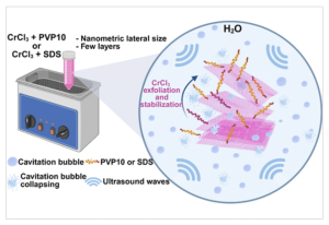
Chromium trihalides, like CrCl3, are part of an emerging class of van der Waals materials that have been showing promise for their magnetic properties. However, CrCl3 has been produced only by mechanical tape exfoliation, a low yield method, and by liquid exfoliation in organic solvents, with a negative impact on the environment and human health. Here, CrCl3 was produced for the first time by liquid-phase exfoliation (LPE) in aqueous medium, in the presence of polyvinylpyrrolidone (PVP10) or sodium dodecyl sulfate (SDS), followed by ultrasonication. It was also the first time that CrCl3 was obtained with nanometric size (<100 nm), and its photothermal, magnetic, and water stability performances were studied. Results showed that CrCl3 + SDS (zeta potential = −19.9 mV) had better water stability than CrCl3 + PVP10 (zeta potential = 8.6 mV). CrCl3 + SDS and CrCl3 + PVP10 were obtained with a mean particle lateral size of 39.4 ± 15.9 and 65.6 ± 47.4 nm and a mean thickness of 4.4 ± 3.9 and 7.1 ± 5.3 nm, respectively. Both materials revealed a similar ability to convert near-infrared light into heat, showing a temperature increase of 4.7 °C (CrCl3 + SDS) and 5.8 °C (CrCl3 + PVP10) after 30 min of irradiation. Results show that the presence of SDS during production leads to a loss of Cl atoms when compared to PVP10, but crystallinity is preserved. Magnetometry measurements show a Néel temperature of 15 K ± 2.0 K for both samples, showing its antiferromagnetism. A Curie–Weiss analysis indicates a ferromagnetic dominant paramagnetic phase due to the positive Curie–Weiss temperatures, with the calculated effective moments as 4.20 μB ± 0.63 μB and 3.95 μB ± 0.49 μB for CrCl3 + PVP10 and CrCl3 + SDS, respectively. These results show that LPE of CrCl3 with PVP10 or SDS produces 2D CrCl3, preserving crystallinity and magnetic properties, and demonstrating potential for spintronic applications.
Find the link here:
https://doi.org/10.1021/acsanm.5c01733

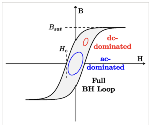
On-chip integration of inductors and transformers can enable power converters with high frequency, high control bandwidth, and low interconnect loss for high-current computing applications. Nevertheless, depositing high-quality magnetic materials that are back end of line compatible with complementary metal-oxide-semiconductor (CMOS) technology, affordable (fast deposition), but optimized for these applications is challenging. Nanogranular materials, such as CoZrO, are promising candidates as core materials for on-chip magnetic components due to their low coercivity and high saturation flux density. However, the deposition rates of these materials remain limited, which limits their cost effectiveness. Herein, the high-rate reactive magnetron sputtering process for homogeneous CoZrO coatings with soft magnetic properties at deposition rates 5 times higher compared to literature is presented. An extensive study is presented on the properties of CoZrO including vibration sample magnetometry, transmission electron microscopy, scanning electron microscopy, and X-ray diffraction characterization results. The findings underscore the importance of maintaining elevated Co:O (at%) ratios up to 75:15 and ensuring uniform microstructure to achieve optimal magnetic properties, which are enabled by the closed-loop O2 controller in our sputtering process.
Find the link here: https://advanced.onlinelibrary.wiley.com/doi/full/10.1002/adem.202402626

Voltage-controlled magnetic skyrmion manipulation has emerged as a promising approach for designing high-density and low-power magnetic devices. This paper investigates the potential of magnetic skyrmion manipulation chambers for such devices, focusing on applications in neuromorphic computing systems. Here, a comprehensive analysis of the properties and characteristics of magnetic skyrmions, their manipulation techniques, and their suitability for magnetic devices is presented. The findings suggest that voltage-controlled skyrmion manipulation chambers have significant advantages over conventional technologies for applications such as high-density data storage, low-power spintronic devices, and adaptable neuromorphic computing systems. These advantages stem from the unique properties of skyrmions, including their topological stability, nanoscale dimensions, and efficient manipulation through voltage control. Furthermore, the dynamic rearrangement capabilities of skyrmion manipulation chambers make them ideal for implementing adaptable neuromorphic architectures and low-power skyrmion-based synaptic devices. This study provides a foundation for further research and development in skyrmion manipulation chambers to realize their potential in neuromorphic computing systems.

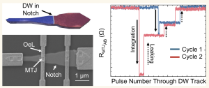
Spiking neural networks seek to emulate biological computation through interconnected artificial neuron and synapse devices. Spintronic neurons can leverage magnetization physics to mimic biological neuron functions, such as integration tied to magnetic domain wall (DW) propagation in a patterned nanotrack and firing tied to the resistance change of a magnetic tunnel junction (MTJ), captured in the domain wall-magnetic tunnel junction (DW-MTJ) device. Leaking, relaxation of a neuron when it is not under stimulation, is also predicted to be
implemented based on DW drift as a DW relaxes to a low energy position, but it has not been well explored or demonstrated in device prototypes. Here, we study DW-MTJ artificial neurons capable of leaky integrate-and-fire (LIF) behavior and demonstrate geometry-dependent leaking dynamics that results in repeatable, tunable LIF operation. Studying the behavior of five different device designs, we show tuning the geometry, stimulating fields and currents, and location ofelectrical contacts results in a wide range ofneuron behavior. Additionally, implementation of an asymmetric notch allows for nonlinear pinning which increased expressivity without sacrificing leaking. The measured behavior is implemented in a simulated spiking neural network that outperforms a 1D model ofcontinuous DW motion and approaches the performance ofan ideal LIF activation function. The results show that the analog LIF capability of DW-MTJ neurons combines many desirable neuron functions into a single device, which can result in varied forms of multifunctional neuromorphic computing.
Find the link here: https://pubs.acs.org/doi/10.1021/acsnano.4c13020?ref=pdf
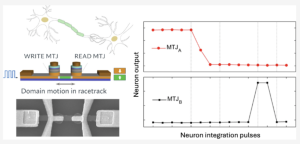
The rich dynamics of magnetic materials makes them promising candidates for neural networks that, like the brain, take advantage of dynamical behaviors to efficiently compute. Here, we experimentally show that integrate-and-fire neurons can be achieved using a magnetic nanodevice consisting of a domain wall racetrack and magnetic tunnel junctions in a way that has reliable, continuous operation over many cycles. We demonstrate the domain propagation in the domain wall racetrack (integration), reading using a magnetic tunnel junction (fire), and reset as the domain is ejected from the racetrack with over 100 continuous cycles. Both the pulse amplitude and pulse number encoding are shown. By simulating a spiking neural network task, we benchmark the performance of the devices against an ideal leaky, integrate-and-fire neuron, showing that the spintronic neuron can match the performance of the ideal. These results achieve demonstration of reliable integrated-fire reset in domain wall-magnetic tunnel junction-based neuron devices for neuromorphic computing.
Find the link here: https://pubs.acs.org/doi/full/10.1021/acs.nanolett.4c05063
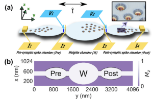
Magnetic skyrmions, as scalable and nonvolatile spin textures, can dynamically interact with fields and currents, making them promising for unconventional computing. This paper presents a neuromorphic device based on skyrmion manipulation chambers to implement spike-timing-dependent plasticity (STDP), a mechanism for unsupervised learning in brain-inspired computing. STDP adjusts synaptic weights based on the timing of pre-synaptic and post-synaptic spikes. The proposed three-chamber design encodes synaptic weight in the number of skyrmions in the center chamber, with left and right chambers for pre- and post-synaptic spikes, respectively. Micromagnetic simulations demonstrate that the timing between applied currents across the chambers controls the final skyrmion count (weight). The device exhibits adaptability and learning capabilities by manipulating chamber parameters, mimicking Hebbian and dendritic location-based plasticity. The device’s ability to maintain state post-write highlights its potential for advancing adaptable neuromorphic devices.
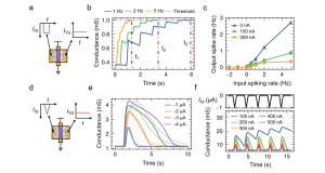
Analog neuromorphic computing systems emulate the parallelism and connectivity of the human brain, promising greater expressivity and energy efficiency compared to those of digital systems. Though many devices have emerged as candidates for artificial neurons and artificial synapses, there have been few device candidates for artificial dendrites. In this work, we report on biocompatible graphene-based artificial dendrites (GrADs) that can implement dendritic processing. By using a dual side-gate configuration, current applied through a Nafion membrane can be used to control device conductance across a trilayer graphene channel, showing spatiotemporal responses of leaky recurrent, alpha, and Gaussian dendritic potentials. The devices can be variably connected to enable higher-order neuronal responses, and we show through data-driven spiking neural network simulations that spiking activity is reduced by ≤15% without accuracy loss while low-frequency operation is stabilized. This positions the GrADs as strong candidates for energy efficient bio-interfaced spiking neural networks.
Find the link here: https://pubs.acs.org/doi/10.1021/acs.nanolett.4c00739?ref=pdf

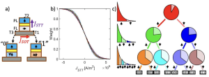
Perpendicular magnetic tunnel junction (pMTJ)-based true-random number generators (RNGs) can consume orders of magnitude less energy per bit than CMOS pseudo-RNGs. Here, we numerically investigate with a macrospin Landau–Lifshitz-Gilbert equation solver the use of pMTJs driven by spin–orbit torque to directly sample numbers from arbitrary probability distributions with the help of a tunable probability tree. The tree operates by dynamically biasing sequences of pMTJ relaxation events, called ‘coinflips’, via an additional applied spin-transfer-torque current. Specifically, using a single, ideal pMTJ device we successfully draw integer samples on the interval [0, 255] from an exponential distribution based on p-value distribution analysis. In order to investigate device-to-device variations, the thermal stability of the pMTJs are varied based on manufactured device data. It is found that while repeatedly using a varied device inhibits ability to recover the probability distribution, the device variations average out when considering the entire set of devices as a ‘bucket’ to agnostically draw random numbers from. Further, it is noted that the device variations most significantly impact the highest level of the probability tree, with diminishing errors at lower levels. The devices are then used to draw both uniformly and exponentially distributed numbers for the Monte Carlo computation of a problem from particle transport, showing excellent data fit with the analytical solution. Finally, the devices are benchmarked against CMOS and memristor RNGs, showing faster bit generation and significantly lower energy use.
Find the link here:
https://iopscience.iop.org/article/10.1088/1361-6528/ad3b01

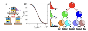
Perpendicular magnetic tunnel junction (pMTJ)-based true-random number generators (RNGs) can consume orders of magnitude less energy per bit than CMOS pseudo-RNGs. Here, we numerically investigate with a macrospin Landau–Lifshitz-Gilbert equation solver the use of pMTJs driven by spin–orbit torque to directly sample numbers from arbitrary probability distributions with the help of a tunable probability tree. The tree operates by dynamically biasing sequences of pMTJ relaxation events, called ‘coinflips’, via an additional applied spin-transfertorque current. Specifically, using a single, ideal pMTJ device we successfully draw integer samples on the interval [0, 255] from an exponential distribution based on p-value distribution analysis. In order to investigate device-to-device variations, the thermal stability of the pMTJs are varied based on manufactured device data. It is found that while repeatedly using a varied device inhibits ability to recover the probability distribution, the device variations average out when considering the entire set of devices as a ‘bucket’ to agnostically draw random numbers from. Further, it is noted that the device variations most significantly impact the highest level of the probability tree, with diminishing errors at lower levels. The devices are then used to draw both uniformly and exponentially distributed numbers for the Monte Carlo computation of a problem from particle transport, showing excellent data fit with the analytical solution. Finally, the devices are benchmarked against CMOS and memristor RNGs, showing faster bit generation and significantly lower energy use.
Find the link here:
https://doi.org/10.1088/1361-6528/ad3b01

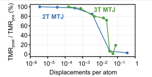
Domain-wall magnetic tunnel junctions (MTJs) are a new spintronic device family that may be exploited in resilient edge logic processors or neuromorphic edge accelerators in the future. Here, domain-wall MTJ logic devices were exposed to large total ionizing doses (TIDs), heavy ion displacement damage, or both. The parts demonstrated complete resilience to the ionizing radiation, but ion-irradiated parts followed a similar degradation curve to previously tested tunnel junction parts in response to heavy ion irradiation. Microscopy and spectroscopy methods confirm significant damage in some devices.
Find the link here:
https://doi.org/10.1109/TNS.2023.3333819


In the ‘Beyond Moore’s Law’ era, with increasing edge intelligence, domain-specific computing embracing unconventional approaches will become increasingly prevalent. At the same time, adopting a variety of nanotechnologies will offer benefits in energy cost, computational speed, reduced footprint, cyber resilience, and processing power. The time is ripe for a roadmap for unconventional computing with nanotechnologies to guide future research, and this collection aims to fill that need. The authors provide a comprehensive roadmap for neuromorphic computing using electron spins, memristive devices, two-dimensional nanomaterials, nanomagnets, and various dynamical systems. They also address other paradigms such as Ising machines, Bayesian inference engines, probabilistic computing with p-bits, processing in memory, quantum memories and algorithms, computing with skyrmions and spin waves, and brain-inspired computing for incremental learning and problem-solving in severely resource-constrained environments. These approaches have advantages over traditional Boolean computing based on von Neumann architecture. As the computational requirements for artificial intelligence grow 50 times faster than Moore’s Law for electronics, more unconventional approaches to computing and signal processing will appear on the horizon, and this roadmap will help identify future needs and challenges. In a very fertile field, experts in the field aim to present some of the dominant and most promising technologies for unconventional computing that will be around for some time to come. Within a holistic approach, the goal is to provide pathways for solidifying the field and guiding future impactful discoveries.
Find the link here: https://iopscience.iop.org/article/10.1088/2399-1984/ad299a

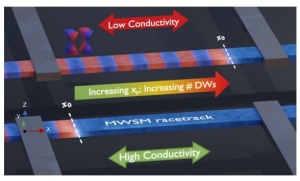
In this paper, we study the electronic structure of a helically magnetized magnetic Weyl semimetal and propose a multistate memory device utilizing the transport in such a magnetic superlattice. For both Bloch- and Néel-type spiral magnetic textures, we report magnetization-tunable flat bands in the superlattice direction via the onset of bulk axial Landau levels (LLs), find the analytic zeroth axial LL wave functions and energy spectrum of both systems, and determine a condition for band flattening. We show that both Bloch- and Néel-type devices using this electronic structure have application in neuromorphic memristive devices and do not rely on the topology or spin polarization of the contacts, with Bloch-type devices allowing for an additional chirality filtering for next-generation computing and memory.
Find the link here: https://journals.aps.org/prb/abstract/10.1103/PhysRevB.109.115159

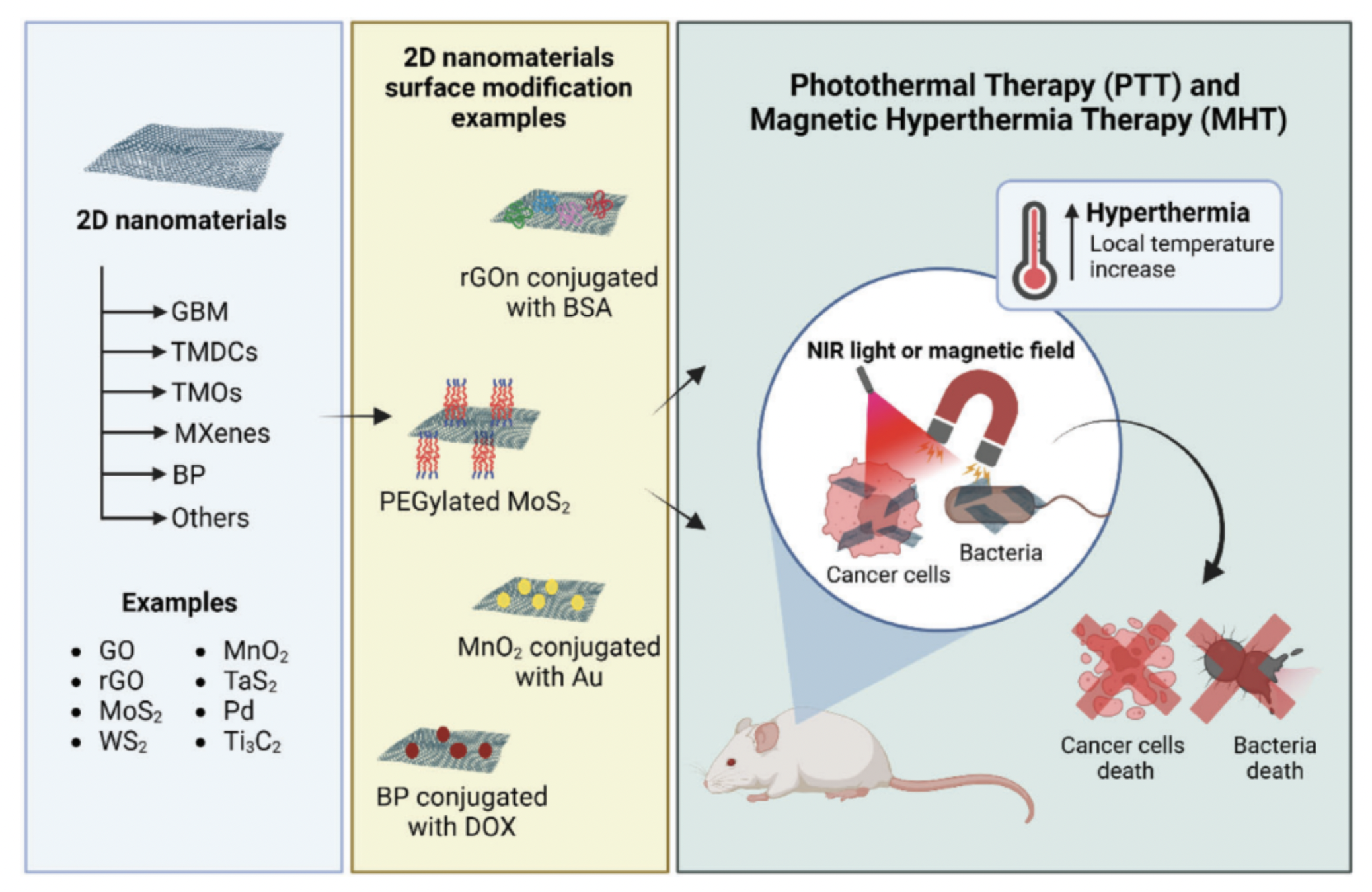
Photothermal therapy (PTT) and magnetic hyperthermia therapy (MHT) using 2D nanomaterials (2DnMat) have recently emerged as promising alternative treatments for cancer and bacterial infections, both important global health challenges. The present review intends to provide not only a comprehensive overview, but also an integrative approach of the state-of-the-art knowledge on 2DnMat for PTT and MHT of cancer and infections. High surface area, high extinction coefficient in near-infra-red (NIR) region, responsiveness to external stimuli like magnetic fields, and the endless possibilities of surface functionalization, make 2DnMat ideal platforms for PTT and MHT. Most of these materials are biocompatible with mammalian cells, presenting some cytotoxicity against bacteria. However, each material must be comprehensively characterized physiochemically and biologically, since small variations can have significant biological impact. Highly efficient and selective in vitro and in vivo PTTs for the treatment of cancer and infections are reported, using a wide range of 2DnMat concentrations and incubation times. MHT is described to be more effective against bacterial infections than against cancer therapy. Despite the promising results attained, some challenges remain, such as improving 2DnMat conjugation with drugs, understanding their in vivo biodegradation, and refining the evaluation criteria to measure PTT or MHT effects.
Find the link here: https://doi.org/10.1002/smll.202306137

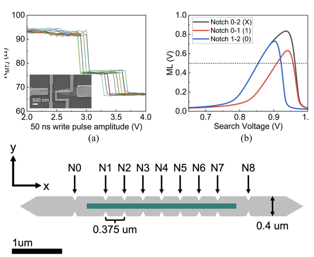
With the rise in in-memory computing architectures to reduce the compute-memory bottleneck, a new bottleneck is present between analog and digital conversion. Analog contentaddressable memories (ACAM) are being recently studied for in-memory computing to efficiently convert between analog and digital signals. Magnetic memory elements such as magnetic tunnel junctions (MTJs) could be useful for ACAM due to their low read/write energy and high endurance, but MTJs are usually restricted to digital values. The spin orbit torque-driven domain wall-magnetic tunnel junction (DW-MTJ) has been recently shown to have multi-bit function. Here, an ACAM circuit is studied that uses two domain wall-magnetic tunnel junctions (DW-MTJs) as the analog storage elements. Prototype DW-MTJ data is input into the magnetic ACAM (MACAM) circuit simulation, showing ternary CAM function. Device-circuit co-design is carried out, showing that 8-10 weight bits are achievable, and that designing asymmetrical spacing of the available DW positions in the device leads to evenly spaced ACAM search bounds. Analyzing available spin orbit torque materials shows platinum provides the largest MACAM search bound while still allowing spin orbit torque domain wall motion, and that the circuit is optimized with minimized MTJ resistance, minimized spin orbit torque material resistance, and maximized tunnel magnetoresistance. These results show the feasibility of using DW-MTJs for MACAM and provide design parameters.
Find the link here: https://doi.org/10.1109/TNANO.2023.3343667

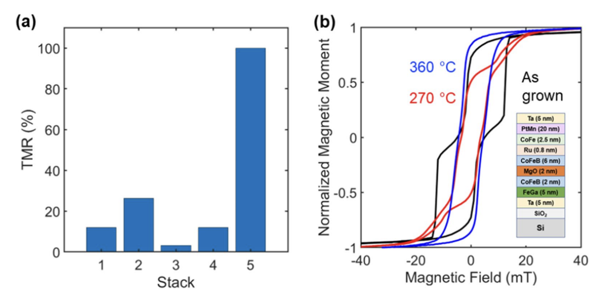
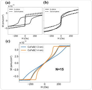
Mechanical strain provides a knob for controlling the magnetization of the magnetostrictive-free layer of magnetic tunnel junctions (MTJs), with many applications for energy-efcient memory and computing. This requires integrating materials with high magnetostriction coefcient into MTJs, while still preserving the CoFeB-MgO tunnel barrier for high tunnel magnetoresistance (TMR). One way to accomplish this is to replace the CoFeB free layer of the MTJ with an exchange-coupled bilayer of CoFeB and a highly magnetostrictive ferromagnet like Galfenol (FeGa). Here, FeGa, a thermally stable magnetostrictive material, is integrated into CoFeB-based MTJs. We show that engineering a thin layer of CoFeB and FeGa provides a means of controlling the magnetic properties and switching feld in FeGa-based MTJs, and that the exchange-coupled FeGa-CoFeB layer can be used as both a free layer and a fxed layer in the MTJ stack with TMR as high as 100%.
Find the link here: https://doi.org/10.1557/s43578-023-01226-z

