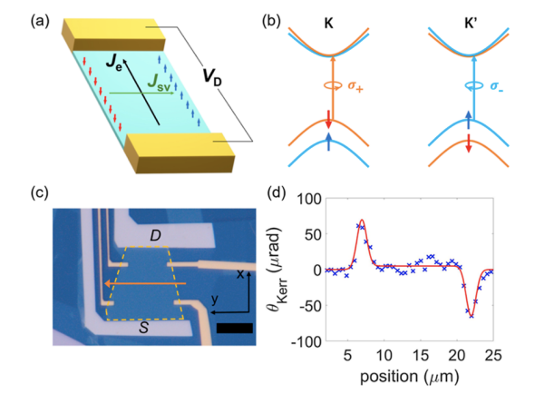
Heavy metal-based two-dimensional van der Waals materials have a large, coupled spin and valley Hall effect (SVHE) that has potential use in spintronics and valleytronics. Optical measurements of the SVHE have largely been performed below 30 K, and understanding of the SVHE-induced spin/valley polarizations that can be electrically generated is limited. Here, we study the SVHE in monolayer p-type tungsten diselenide (WSe2). Kerr rotation (KR) measurements show the spatial distribution of the SVHE at different temperatures, its persistence up to 160 K, and that it can be electrically modulated via gate and drain bias. A spin/valley drift and diffusion model together with a reflection measurement and a four-port electrical measurement is used to interpret the KR data. A lower-bound spin/valley lifetime is predicted to be of 40 ns and a mean free path of 240 nm below 90 K, 2 orders of magnitude higher than a previous work that uses similar methods. The spin/valley polarization on the edge is calculated to be ∼4% at 45 K. These results are important steps toward practical use of the SVHE.
Find the link here: https://pubs.acs.org/action/showCitFormats?doi=10.1021/acsaelm.2c00599&ref=pdf


CMOS-based computing systems that employ the von Neumann architecture
are relatively limited when it comes to parallel data storage and processing. In
contrast, the human brain is a living computational signal processing unit that
operates with extreme parallelism and energy efficiency. Although numerous
neuromorphic electronic devices have emerged in the last decade, most of
them are rigid or contain materials that are toxic to biological systems. In this
work, we report on biocompatible bilayer graphene-based artificial synaptic
transistors (BLAST) capable of mimicking synaptic behavior. The BLAST
devices leverage a dry ion-selective membrane, enabling long-term potentia-
tion, with ~50 aJ/μm2 switching energy efficiency, at least an order of magni-
tude lower than previous reports on two-dimensional material-based artificial
synapses. The devices show unique metaplasticity, a useful feature for gen-
eralizable deep neural networks, and we demonstrate that metaplastic BLASTs
outperform ideal linear synapses in classic image classification tasks. With
switching energy well below the 1 fJ energy estimated per biological synapse,
the proposed devices are powerful candidates for bio-interfaced online
learning, bridging the gap between artificial and biological neural networks.
Find the link here: https://www.nature.com/articles/s41467-022-32078-6

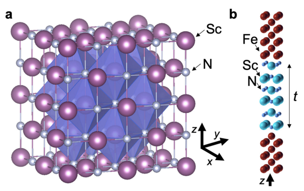
The state-of-the-art magnetic tunnel junction, a cornerstone of spintronic devices and circuits, uses a magnesium oxide tunnel barrier that provides a uniquely large tunnel magnetoresistance at room temperature. However, the wide bandgap and band alignment of magnesium oxide-iron systems increases the resistance-area product and creates variability and breakdown challenges. Here, the authors study using first principles narrower-bandgap scandium nitride (ScN) transport properties in magnetoresistive junctions in comparison to magnesium oxide. The results show a high magnetoresistance in Fe/ScN/Fe via Δ1and Δ2′ symmetry filtering with low wave function decay rates, suggesting scandium nitride could be a new barrier material for spintronic devices.
Find the link here: https://doi.org/10.1002/adts.202100309

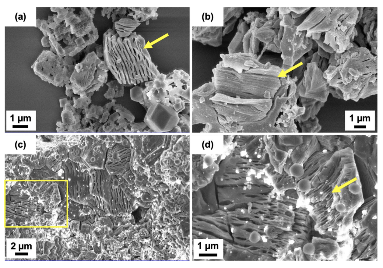
MXenes are a large class of materials that are chemically exfoliated from metal–aluminum–carbon (MAX) bulk crystals into low-dimensional sheets. While many MXenes have been theoretically predicted, the careful balance required in the exfoliation between breaking the inter-layer bonds without damaging the intra-layer bonds of the sheets has limited synthesis and experimental study. Here, we developed the synthesis of Cr2C from its parent Cr2AlC MAX phase and showed the etching is optimized using sodium fuoride and hydrogen chloride with a modifed minimally intensive layer delamination (mMILD) method in a cold environment of 9 °C. We further optimized the intercalation and delamination using sonication and washing methods. The resulting Cr2C crystal structure was characterized. These results open up Cr2C to experimental study, including of its predicted emergent magnetic properties, and develop guidelines for synthesizing new MXene materials.
Find the link here: https://link.springer.com/article/10.1557/s43578-021-00258-7

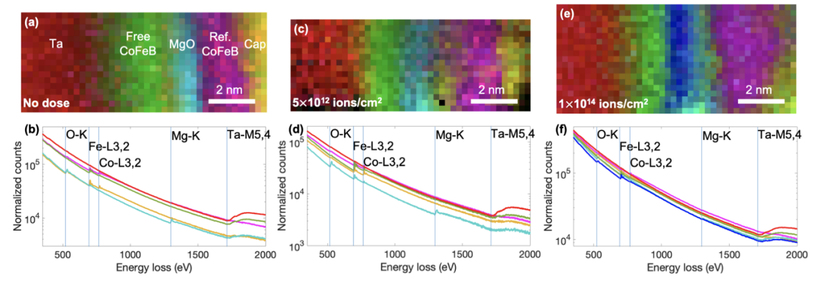
We study the impact of irradiation on magnetic tunnel junction (MTJ) films with perpendicular magnetic anisotropy (PMA) and spin-orbit torque (SOT) switching using magneto-optical Kerr effect and transmission electron microscopy. Our results show that the thin-film stack is robust to gamma ionizing dose up to 1 Mrad(Si) and Ta 1+ ion irradiation fluences up to 10 12 ions/cm 2 , showing SOT PMA MTJs are radiation-hard. But, at very high Ta 1+ ion irradiation between 10 12 and 10 14 ions/cm 2 , reduced coercivity and eventually greatly reduced PMA are observed, corresponding with an increase in intermixing of the CoFeB-MgO layers, particularly at the lower CoFeB-MgO interface. These results agree with displacement damage modeling that predicts higher damage in the layers closer to the bottom heavy metal and substrate. Compared to spin transfer torque and in-plane anisotropy MTJs, needing a top-pinned stack, a thicker heavy metal layer, and perpendicular anisotropy that is pinned out of plane by interfaces, all could make SOT PMA MTJs more susceptible to damage at high doses.
Find the link here: https://ieeexplore.ieee.org/document/9378556

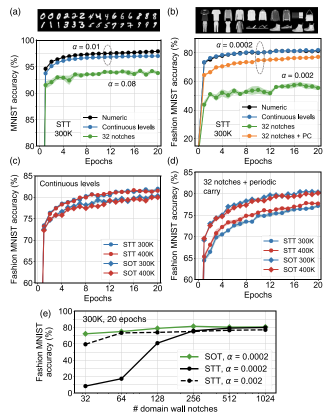
Inspired by the parallelism and efficiency of the brain, several candidates for artificial synapse devices have been developed for neuromorphic computing, yet a nonlinear and asymmetric synaptic response curve precludes their use for backpropagation, the foundation of modern supervised learning. Spintronic devices—which benefit from high endurance, low power consumption, low latency, and CMOS compatibility—are a promising technology for memory, and domain-wall magnetic tunnel junction (DW-MTJ) devices have been shown to implement synaptic functions such as long-term potentiation and spike-timing dependent plasticity. In this work, we propose a notched DW-MTJ synapse as a candidate for supervised learning. Using micromagnetic simulations at room temperature, we show that notched synapses ensure the non-volatility of the synaptic weight and allow for highly linear, symmetric, and reproducible weight updates using either spin transfer torque (STT) or spin–orbit torque (SOT) mechanisms of DW propagation. We use lookup tables constructed from micromagnetics simulations to model the training of neural networks built with DW-MTJ synapses on both the MNIST and Fashion-MNIST image classification tasks. Accounting for thermal noise and realistic process variations, the DW-MTJ devices achieve classification accuracy close to ideal floating-point updates using both STT and SOT devices at room temperature and at 400 K. Our work establishes the basis for a magnetic artificial synapse that can eventually lead to hardware neural networks with fully spintronic matrix operations implementing machine learning.
Find the link here: https://aip.scitation.org/doi/10.1063/5.0046032

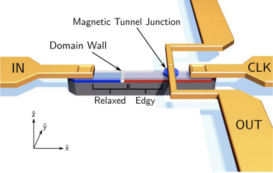
Neuromorphic computing with spintronic devices has been of interest due to the limitations of CMOS-driven von Neumann computing. Domain wall-magnetic tunnel junction (DW-MTJ) devices have been shown to be able to intrinsically capture biological neuron behavior. Edgy-relaxed behavior, where a frequently firing neuron experiences a lower action potential threshold, may provide additional artificial neuronal functionality when executing repeated tasks. In this letter, we demonstrate that this behavior can be implemented in DW-MTJ artificial neurons via three alternative mechanisms: shape anisotropy, magnetic field, and current-driven soft reset. Using micromagnetics and analytical device modeling to classify the Optdigits handwritten digit dataset, we show that edgy-relaxed behavior improves both classification accuracy and classification rate for ordered datasets while sacrificing little to no accuracy for a randomized dataset. This letter establishes methods by which artificial spintronic neurons can be flexibly adapted to datasets.


There are pressing problems with traditional computing, especially for accomplishing data-intensive and real-time tasks, that motivate the development of in-memory computing devices to both store information and perform computation. Magnetic tunnel junction memory elements can be used for computation by manipulating a domain wall, a transition region between magnetic domains, but the experimental study of such devices has been limited by high current densities and low tunnel magnetoresistance. Here, we study prototypes of three-terminal domain wall-magnetic tunnel junction in-memory computing devices that can address data processing bottlenecks and resolve these challenges by using perpendicular magnetic anisotropy, spin–orbit torque switching, and an optimized lithography process to produce average device tunnel magnetoresistance TMR = 171% and average resistance-area product RA = 29 𝛺𝜇m2Ω μm2, close to the RA of the unpatterned film. Device initialization variation in switching voltage is shown to be curtailed to 7%–10% by controlling the domain wall initial position, which we show corresponds to 90%–96% accuracy in a domain wall-magnetic tunnel junction full adder simulation. Repeatability of writing and resetting the device is shown. A circuit shows an inverter operation between two devices, showing that a voltage window is large enough, compared to the variation noise, to repeatably operate a domain wall-magnetic tunnel junction circuit. These results make strides in using magnetic tunnel junctions and domain walls for in-memory and neuromorphic computing applications.
Find the link here: https://aip.scitation.org/doi/10.1063/5.0038521

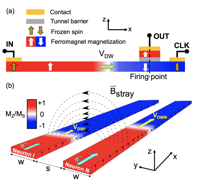
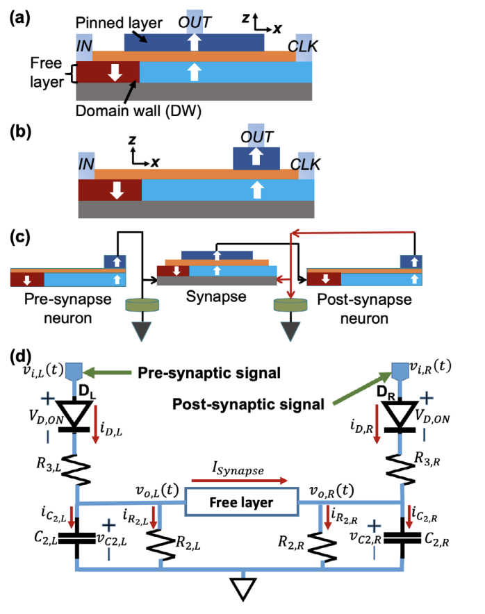
There have been recent efforts towards the development of biologically-inspired neuromorphic devices and architecture. Here, we show a synapse circuit that is designed to perform spike-timing-dependent plasticity which works with the leaky, integrate, and fire neuron in a neuromorphic computing architecture. The circuit consists of a three-terminal magnetic tunnel junction with a mobile domain wall between two low-pass filters and has been modeled in SPICE. The results show that the current flowing through the synapse is highly correlated to the timing delay between the pre-synaptic and post-synaptic neurons. Using micromagnetic simulations, we show that introducing notches along the length of the domain wall track pins the domain wall at each successive notch to properly respond to the timing between the input and output current pulses of the circuit, producing a multi-state resistance representing synaptic weights. We show in SPICE that a notch-free ideal magnetic device also shows spike-timing dependent plasticity in response to the circuit current. This work is key progress towards making more bio-realistic artificial synapses with multiple weights, which can be trained online with a promise of CMOS compatibility and energy efficiency.
Find the link here: https://iopscience.iop.org/article/10.1088/1361-6463/ab4157

